
New method creates nanoscale patterns on hard material at room temperature, can boost chip-making
TL;DR AI
2 min readKey summary
Researchers demonstrated a room-temperature, one-step method to pattern hard chip materials with aligned nanoscale wrinkles.
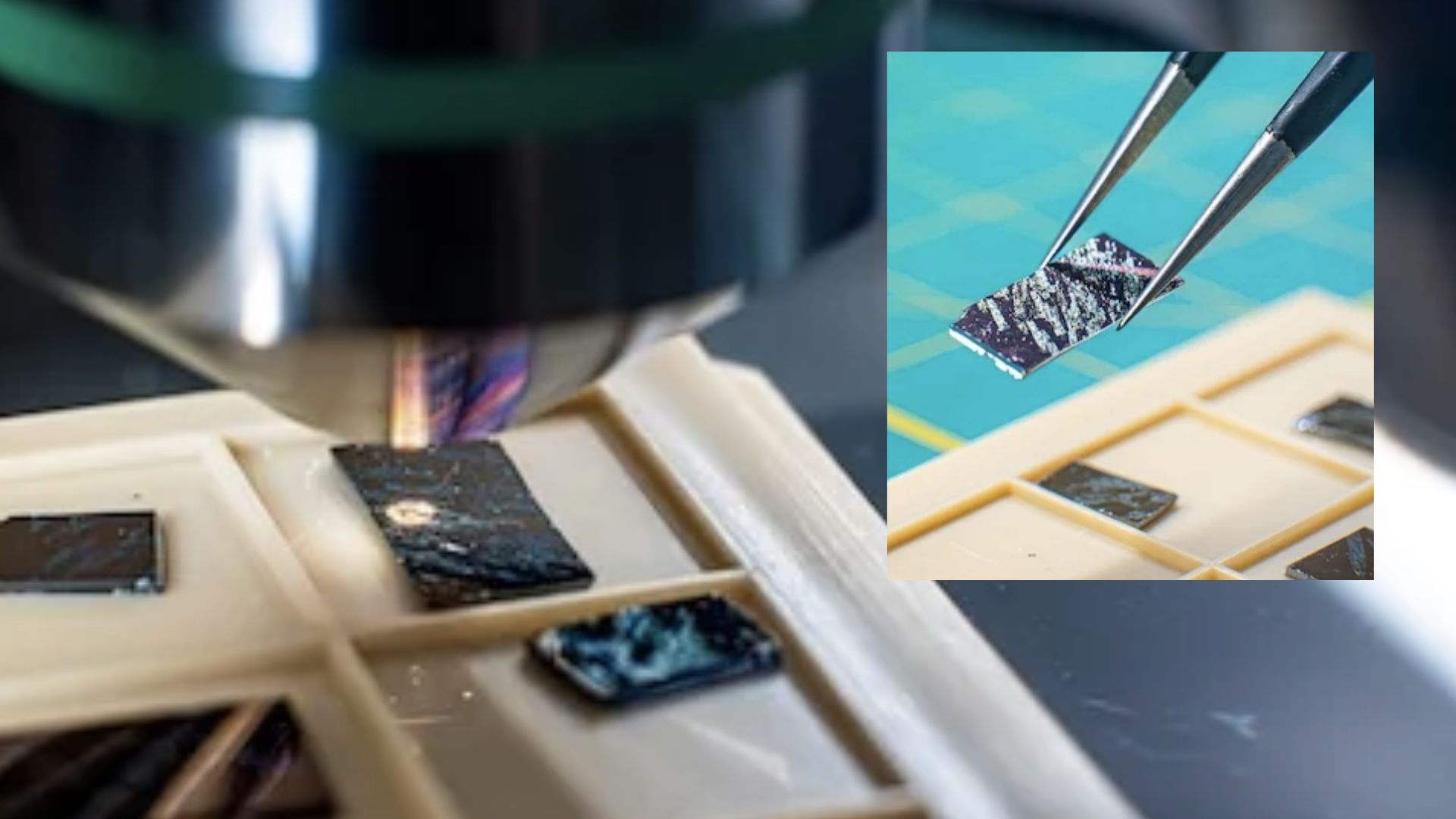
The team used an anisotropic alpha-molybdenum trioxide layer and an electron beam to imprint patterns on silica and other insulators.
After patterning, the temporary layer was peeled away, leaving structures on rigid substrates without conventional multi-step processing.
The approach could simplify manufacturing of optical and electronic components such as gratings and photonic devices, cutting cost and complexity.